


Blog
Scientists Have a New Way to Gauge the Growth Of Nanowires
Scientists devise new method to measure the growth of the nanowires
Scientists have discovered two distinct kinds of defects in the individual nanowires which aren’t much bigger than a diameter of human hair but offers great insight. This discovery was made by the researchers from the Brookhaven National Laboratories and the U.S. Department of Energy while conducting their won study. The nanowires used in this study were made up of indium gallium arsenide.
The new age optoelectronics
It is worth noting that these nanowires possess such a vast amount of future application potential and that the scientists have to create a new term to define their potential as “optoelectronics”. Optoelectronics can be defined as such devices which can work through actively converting the light energy into electrical impulses. A prime example of the optoelectronics is the wide spread use of the fiber optic relays to boost the internet connectively globally. However, a major issue with the optoelectronics their effectiveness and performance can easily take a hit even with a tiny defect found within its components.
The worse thing about the defects is that it can result in causing a dramatic change in the optical as well as electronic properties of the materials used in the devices. Therefore scientists are looking closely into the development of the optoelectronics which can help in enhancing and tailoring the functionality of the optoelectronics in the future which is feasible only through using such materials which has the ability to successfully manipulate the quantum information stored upon it.
Understanding the defects
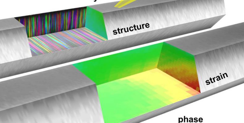
Scientists have started understanding the defects in the nanowires using a new technique called Bragg ptychography which essentially helps in observing the defects within its operating environment. It wasn’t possible earlier but having such an ability in hand allows them to describe how these particular defects present in nanowire will affect it as the device as whole in the future. Scientists even claim that understanding the defects in nanowires also offers a missing link which was present between the nano scale defect structure and the strain present at varied points in the nanowires.This also offers a chance to have a better control over the optoelectronic properties of the nanowires used within any such device.
How Bragg ptychography works?
Using this technique scientists shine an X-ray beam on materials at the overlapping spots whereby the beam is slowly moves all across the stage. The atoms scattered from the X rays generated information which is then seen in a three dimensional view of the nanowires or material at hand. The three dimensional images created by the X rays is extremely detailed to the so called atomic resolution. This technique was employed at Brookhaven’s hard X-ray nano probe.
Quite recently scientists have come up with new algorithms which helps in generating the three dimensional picture with much more improvement by carefully collecting and constructing the grid based information from the X-rays. This method has also become quite flexible over the time thereby allowing researchers to exclusively illuminate the smaller features on the nanowires to a very smaller spot size.
